Delay in CMOS Integrated Circuits
This article introduces transient response analysis, RC delay model, Elmore delay device sizing and strategies to optimize timing in transistor level.
Introduction
We begin with a few definitions illustrated in the next figure:
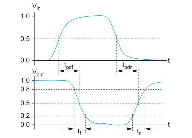
- Propagation delay time, tpd = maximum time from the input crossing 50% to the output crossing 50%.
- Contamination delay time, tcd = minimum time from the input crossing 50% to the output crossing 50%.
- Rise time, tr = time for a waveform to rise from 20% to 80% of its steady-state value.
- Fall time, tf = time for a waveform to fall from 80% to 20% of its steady-state value.
- Edge rate, trf = (tr + tf) / 2.
A timing analyzer computes the arrival times at each node and checks that the outputs arrive by their required time. The slack is the difference between the required and arrival times. Positive slack means that the circuit meets timing. Negative slack means that the circuit is not fast enough.
Transient response analysis
Transient response analysis is based on charging or discharging of the capacitances in the circuit. First of all, we need to figure out all the capacitances in a transistor. Let us use two inverters in series as an example:
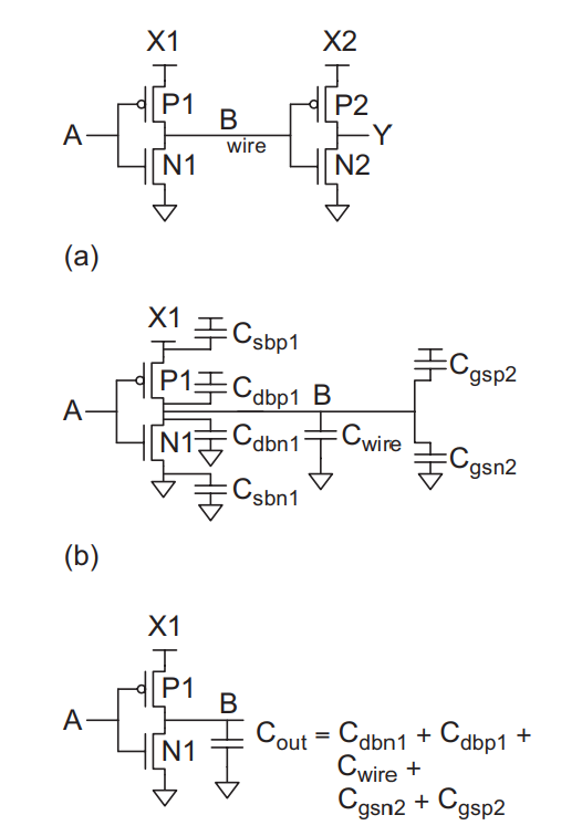
The gate capacitance of the transistors in X1 and the diffusion capacitance of the transistors in X2 do not matter because they do not connect to node B. We only care the diffusion capacitance of X1, the gate capacitance of X2 and the wire capacitance when we are considering the node B.
Suppose the transistors obey the long-channel models, when the voltage step arrives, we can analyse transient response as follows:
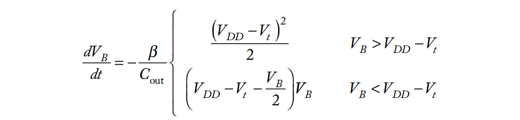
During saturation, the current is constant and VB drops linearly until it reaches VDD-Vt. After entering triode region, the differential equation becomes nonlinear.
In a real circuit, the input comes from another gate with a nonzero rise/fall time. This input can be approximated as a ramp with the same rise/fall time. We can also analyse transient response as follows:
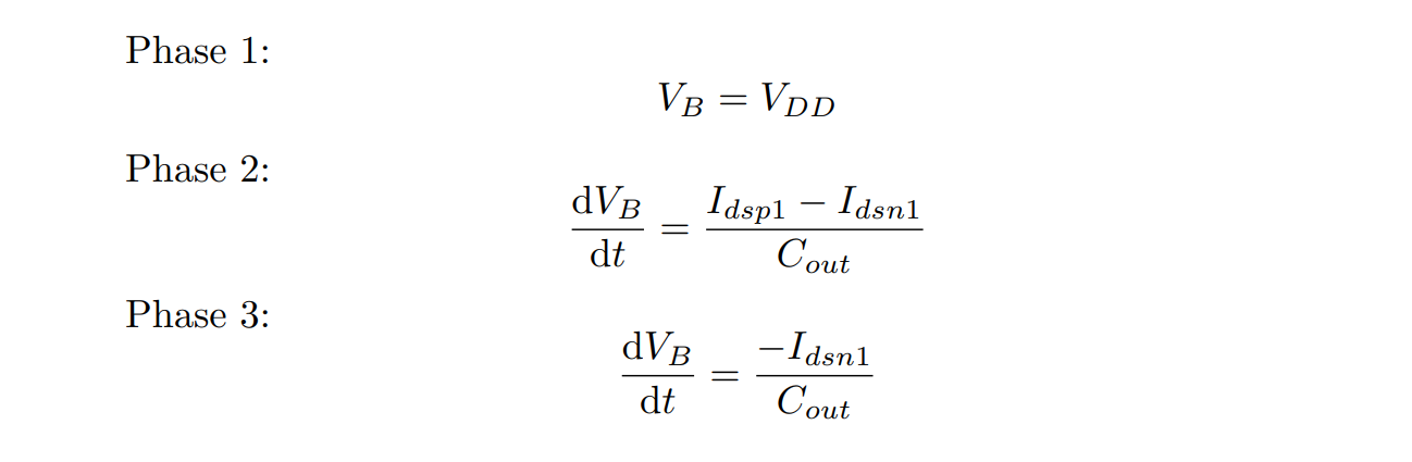
- Phases 1 is when NMOSFET is closed and PMOSFET is on.
- Phases 2 is when both NMOSFET and PMOSFET is on.
- Phases 3 is when PMOSFET is closed and NMOSFET is on.
The differential equations used the long-channel model for transistor current, which is inaccurate in modern processes. And also, they become much complicated when the scale of circuit is large. Therefore, we need to find simplified morels that offer more insight and tolerable accuracy.
RC delay model
The RC delay model treats a transistor as a switch in series with a resistor.
Firstly, let’s take some things into consideration:
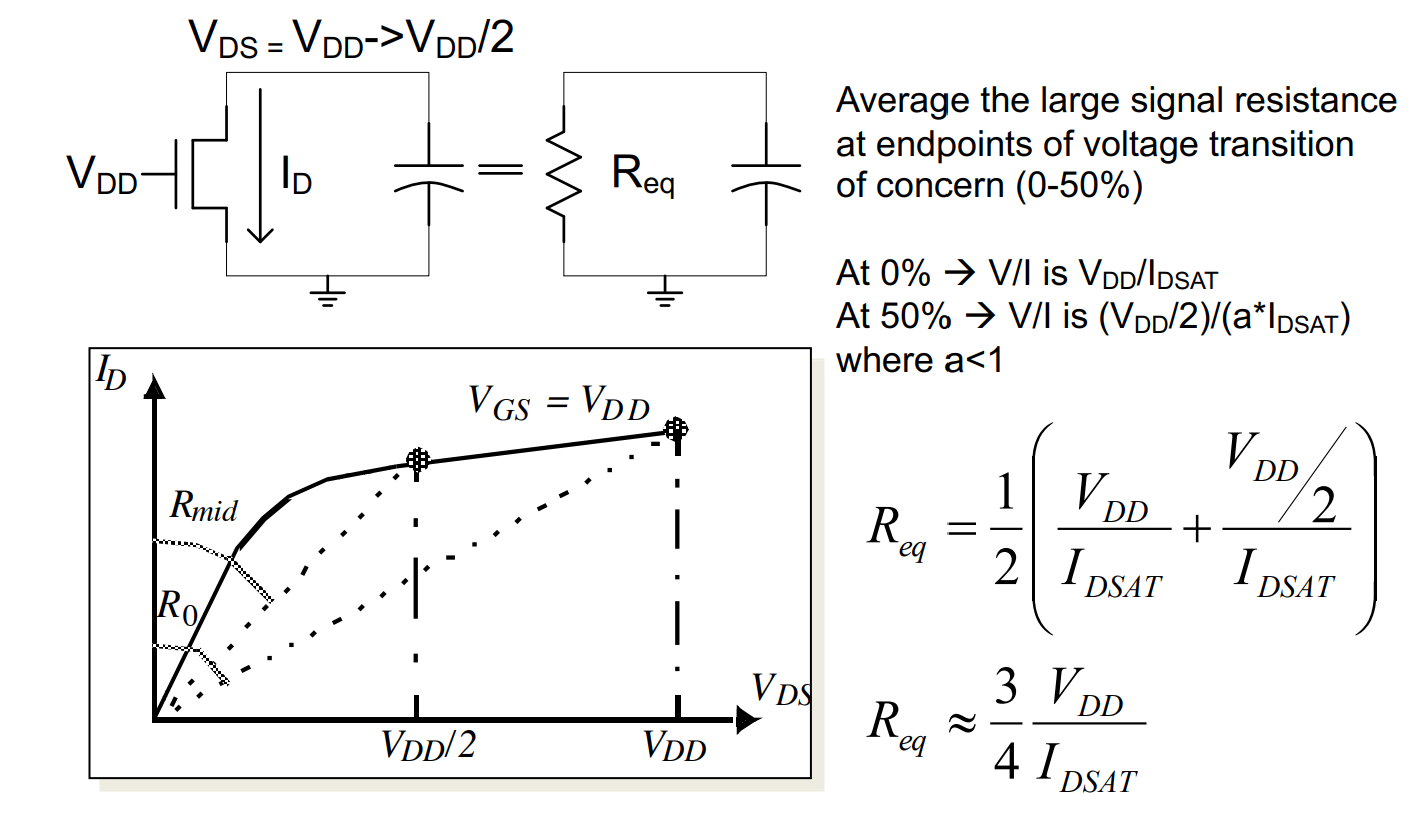
- The effective resistance is the ratio of Vds to Ids averaged across the switching interval of interest.
- A MOS transistor of k times unit width has resistance R/k because it delivers k times as much current. Similarly, it has gate capacitance kC because tof the area is k times larger.
- A unit pMOS transistor has greater resistance, generally in the range of 2R–3R, because of its lower mobility.
According to the long-channel model, the current Id decreases linearly with channel length. That’s why a MOS transistor of k times unit width has resistance R/k. However, if a transistor is fully velocity-saturated, current and resistance become independent of channel length. In manually calculation, we ignore this situation for simplicity but we need to recognize that series transistors will be somewhat faster than predicted.
Effective resistance
Gate capacitance and parasitic capacitance
Increase the width of the transistor will increase both the gate capacitance and diffusion capacitance proportionally, but increasing channel length increases gate capacitance proportionally but does not affect diffusion capacitance.
Although capacitances have a nonlinear voltage dependence, we use a single average value.
Simplified RC circuit
We can simply take transistor as a first-order RC network.
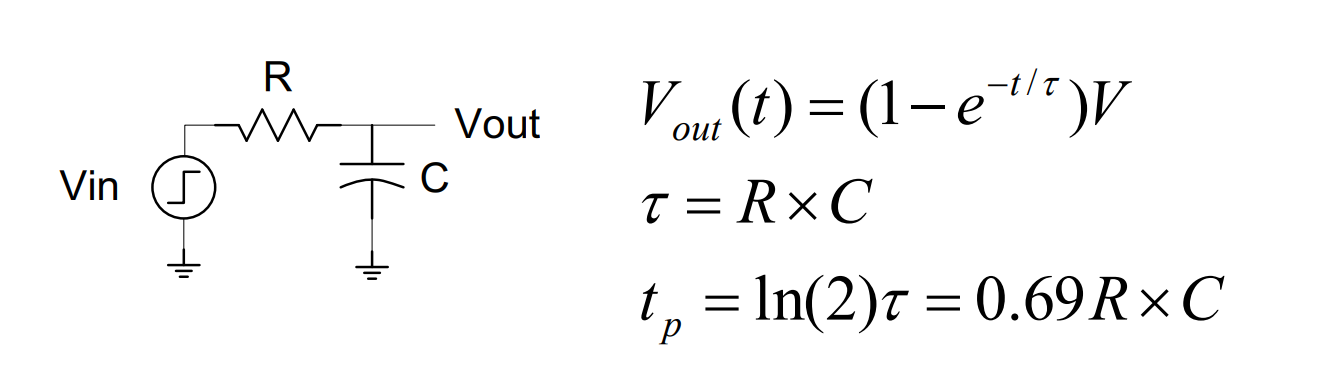
Even for series transistors, we can also use first-order RC network to model cause the error in estimated propagation delay from the first-order approximation is less than 7%. Even in the worst case, where the two time constants are equal, the error is less than 15%.
When we consider a node, what we need to take into consideration is the diffusion capacitances of the logic cells before the node and the gate capacitances of the logic cells behind the node. All these capacitances should be connected to the node we are considering.
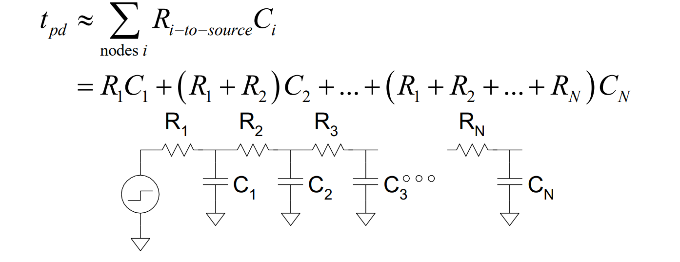
Elmore delay
In general, most circuits of interest can be represented as an RC tree. The Elmore delay model estimates the delay from a source switching to one of the leaf nodes changing as the sum over each node i of the capacitance C in the node, multiplied by the effective resistance Ris on the shared path from the source to the node and the leaf.
What is shared path? Let’s take a 3-input NAND gate as an example.
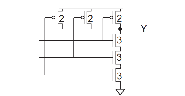
For convenience, the number on the size of the transistor refers to how many times the size of this transistor is the minimum size of an NMOSFET in a specific process. Same to the effective resistances.
if the output is loaded with h identical NAND gates, we can simplify the circuit into RC circuit. The left side is the equivalent circuit including the load for the falling transition in the worst situation, and the right side is for the rising transition in the worst situation.
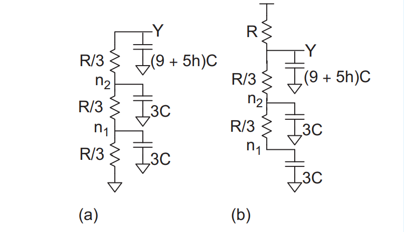
When calculating the Elmore delay of the falling transition, the shared path is the path from Y to R/3, n2, R/3, n1, R/3 and finally ground. Therefore, we have:
tpdf = (3C)(R/3) + (3C)(R/3 + R/3) + ((9 + 5h)C)(R/3 + R/3 + R/3) = (12 + 5h)RC
When calculating the Elmore delay of the rising transition, the shared path is the path from Y to R and VDD. These two R/3 resistors are not on the “shared path”. Therefore, we have:
tpdr = (15 + 5h)RC
Device sizing
Since a unit pMOS transistor has greater resistance because of its lower mobility, it is better to change sizes of pMOS transistors to several times of pMOS transistors according to how many times the P-type carriers are more conductive than n-type carriers in a specific process to make tf and tr equal.
If we connect transistors in series, since the current must pass through all transistors, it may be necessary to increase the size of the transistors proportionally to reduce the threshold voltage and increase current driving capability.
If we connect transistors in parallel, since each transistor can operate independently, and the current is distributed among the transistors, there is no need to change the size of the transistors in a parallel connection.
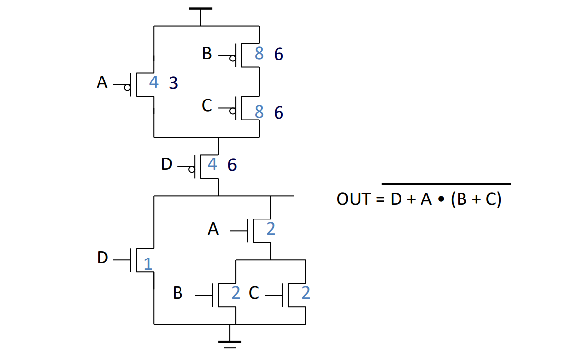
This is a complex example of device sizing. Also, the number on the size of the transistor refers to how many times the size of this transistor is the minimum size of an NMOSFET in a specific process:
Timing optimization in transistor level
- RC delay is dependent to layout.
- In a good layout, diffusion nodes are shared wherever possible to reduce the diffusion capacitance.
- Good placement: short wires & no diffusion routing.
- Use multi-fingered transistors if the width of designed transistor is too large to get less diffusion capacitance.
- Increase transistor sizes – lower R but increase parasitic capacitance. Watch out for self-loading!
- Increase VDD - not usually possible due to reliability and power penalties.
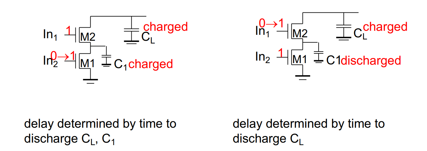
- Delay is dependent on the pattern of inputs. For instance:
Summary
CMOS delay is dictated by many factors. The first-order RC model is sufficient and efficient to estimate the delay of circuit. Computing delays of complex gates is challenging due to input pattern dependency.