From History to Properties,A Quick View of Integrated Circuits and Properties of MOS Transistors as Switches
This article contains a quick view of the history of integrated circuits, the rapid development of this industry, the challenges we are facing and properties of MOS transistors as switches
Preview
In this article, we will first have a brief view of the history of integrated circuits, and introduce structures and properties of MOS transistors as switches. In the following article we will have more in-depth introduction to how transistors actually work, derive the small-signal model of transistors and discuss the secondary effects.
A Brief History
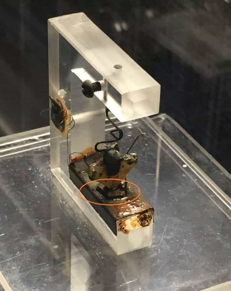
In 1947, John Bardeen and Walter Brattain built the first functioning point contact transistor when working in a group led by physicist William Shockley at Bell Laboratories. The point contact transistor was able to amplify a weak input signal by controlling the flow of a larger output current across the germanium. This was a breakthrough in the field of electronics, as it opened up new possibilities for computing, communication, and technology. Bardeen, Brattain, and their supervisor William Shockley received the Nobel Prize in Physics in 1956 for creating the transistor. An image of the first transistor in the world is shown as Fig 1.1. The sheet of metal in the yellow circle below the metal arrow is the germanium metal.
In 1958, Jack Kilby built the first integrated circuit flip-flop with two transistors at Texas Instruments. Ten years later, he realized that transistors can be integrate in one piece of silicon. He also received Nobel Prize in 2000 for the invention of integrated circuits.
The rapid development and challenges of the integrated circuit industry in the 21st century
In 2022, Apple announced the M2 chip using next-generation 5-nanometer technology with more than 20 billion transistors.The system-on-a-chip (SoC) design of M2 is built using enhanced, second-generation 5-nanometer technology, and consists of 20 billion transistors — 25 percent more than M1. The additional transistors improve features across the entire chip, including the memory controller that delivers 100GB/s of unified memory bandwidth — 50 percent more than M1. [1]. Such a high-speed technological iteration is rarely seen in other industries.
The development comes from the miniaturization of transistors and the improvements of manufacturing processes. According to Moore’s law, the number of transistors on a microchip doubled about every two years, and predicted that this would continue for at least another decade. Competitive pressure drives each company to follow Moore’s Law, making it a self-fulfilling prophecy. In the past few decades, the integration and performance of integrated circuits were constantly improving, which became the cornerstone of emerging technologies, such as high-speed communication network, the internet of things, and artificial intelligence.
Obviously, due to the restriction of physical principles, this scaling cannot go on forever because transistors cannot be smaller than atoms. In fact, the feature size of transistors has reached such a small scale that traditional structure of transistors can not perform well because of the short-channel effects, diffraction limit of planar lithography and bottleneck of energy efficiency. Scientists therefore developed new structures of transistors such as FinFET and has became the dominant gate design at 14 nm, 10 nm and 7 nm process nodes[2].
Although the further progress of chip integration has been challenged, increasing the integration of chips as much as possible is still one of the main means adopted by integrated circuit design and manufacturing enterprises to improve performance of integrated circuits. Many new structures of transistors have been constantly proposed, but it is worth noting that the integrated circuit industry will eventually face the limitations of physical laws. So what is the direction of future development in this industry? No one has a clear answer. Quantum computing may be the breaking point of this tough situation and lead future technological revolution.
MOS Transistors as Switches
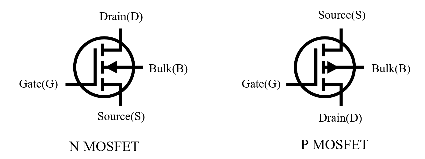
MOS transistors are a type of field-effect transistor (FET) that use a metal-oxide-semiconductor (MOS) structure to control the flow of current between the source and drain terminals. There are four terminals in a single MOS transistor: gate, source, drain and bulk (also called substrate). Most textbooks ignored the substrate terminal when introducing the structure of MOS transistors because in CMOS circuits, the substrate terminal of PMOS is always connected to power and the substrate terminal of NMOS is always connected to ground. However, revealing this terminal will help us have a better understanding of the structures and properties of MOS transistors. In the rest of this article, we assume that the bulk terminal is connected to the source terminal. Typical symbol of MOS transistors is shown as Fig 1.2.
The operation of a MOS transistor depends on the voltage applied to the gate terminal, which creates an electric field that attracts or repels charge carriers in the semiconductor substrate below the oxide layer. For NMOSFET, when the gate voltage is above a certain threshold, an inversion layer of negatively charged carriers forms near the oxide-semiconductor interface, creating a conductive channel between the source and drain. The current flowing through the channel is proportional to the difference between the drain and source voltages, and can be modulated by changing the gate voltage. For PMOSFET, when the gate voltage is below a certain threshold, an electric field is formed, which causes a kind of positively charged carriers called holes (a kind of abstract physical model that doen not exist in real world) in the channel area to flow, causing the circuit to switch on. The current flowing through the channel is similarly proportional to the difference between the source and drain voltages. Therefore, these two types of transistors can be viewed as switches controlled by Vgs. It would be much more complicated if you take a deeper look into the physical principle of transistors cause it involves knowledge of other disciplines including semiconductor physics, quantum physics and structural chemistry, etc. Fortunately, as a VLSI designer, You don’t need to figure out all these principles. What you need to do is just understand properties of transistors and how they work from an engineering perspective.
The turn-on condition of NMOSFET is when the voltage between gate and source (Vgs) is greater than the threshold voltage (Vth). Threshold voltage is a specific voltage value that determines whether the MOSFET turns on or off. Once Vgs is greater than Vth, the NMOS turns on, there will be current flow from drain to the source if you add a voltage between the drain terminal and the source terminal.
The turn-on condition of PMOSFET is when the voltage between gate and source (Vgs) is less than the threshold voltage (Vth). Threshold voltage is a specific voltage value that determines whether the MOSFET turns on or off. Once Vgs is less than Vth, the PMOS turns on, there will be current flow from source to the drain if you add a voltage between the source terminal and the drain terminal.
The conditions for switching on and off are as follows:
| Type | Open Condition | Closed Condition | Current Flow Direction |
|---|---|---|---|
| NMOSFET | Vgs > Vth | Vgs < Vth | From the Drain to the Source |
| PMOSFET | Vgs < Vth | Vgs > Vth | From the Source to the Drain |
Summary
In this article, we discussed the history of integrated circuits, the rapid development of the integrated circuit industry and the challenges faced by the integrated circuit industry in the 21st century, and introduced the properties of MOSFETs as switches. In the following article, we will continue to explore how transistors actually work, derive the small-signal model of transistors and discuss the secondary effects.
References
[1]https://www.apple.com/newsroom/2022/06/apple-unveils-m2-with-breakthrough-performance-and-capabilities/
[2]https://en.wikipedia.org/wiki/Fin_field-effect_transistor